Remove top cover and tubes 3. Star connections for ground and power are always a good practice for audio circuit board layouts.

1500w Power Amplifier Circuit And Components Layout
Other electrolytic can be 10 or 15v.

Amplifier driver board diagram. 35w to 75w stereo amps —tda2050**new**. Stereo amplifier circuit diagram we are going to design here is basically the combination of two mono audio amplifier. A good place to start is with the ground and power circuits design layout.
The driver stage is used to provide a high impedance input to the power amplifier. Heat sink is necessary for the mosfets. 2.53 w for class b and 30.2 w for class a.
But it is recommended to use 5v input for maximum output performance. Imagine you are watching a movie with your family. Bolt the new populated circuit board into the chassis.
50w ocl mosfet amps —using k1058 + j162. Unplug amplifier and let cool if necessary 2. Assemble the circuit on a good quality pcb.
Erh india (pack of 5) pam 8403 amplifier board kit 5v aamplifier board 2 channels 3w dual channel stereo mini class d digital audio power amplifier board. For transistor booster / final transistor using 8 set sanken 2sc2922 and 2sa1216, wiring booster transistor see here : In this video you will see full circuit diagram 500 watt amplifier driver board which was sale by me and most of subscriber had purchased from me.
Circuit diagram for interfacing with two 3w speakers with the pam8403 amplifier board is given below. Here we use a power transistor tip41 in class a mode. (check out the tea2025 datasheet for more information on that) on the input side, you should use a dual potentiometer.
The pam8403 amplifier board can be powered using any voltage ranging from 2.5v to 5v dc. 3.1 demonstration pcb board layout as with all low noise, high quality circuit board layouts, the lm4702 power amplifier driver requires careful consideration. Note the location of input and output resistors on the circuit board and unsolder.
For transistor booster / final transistor using 8 set sanken 2sc2922 and 2sa1216, wiring booster transistor see here : If you want to build this power amp, you can see the. Module 4.3 describes some other amplifier circuits that are commonly used to control the values of input and output impedances in amplifier circuits.
The importance of an amplifier's input and output impedance is discussed in ac theory module 7, and using nfb to control impedance is described in amplifiers module 3.2. For l1 make 12turns of enameled copper wire on a 1cm dia: Build the 9v mini amplifier.
Number and unsolder all wires from the driver board. Make a layout diagram first which very nearly follows the schematic diagram before attempting any soldering. The ramping amplifier control diagram in figure 11 shows a plot
50 watts mosfet amplifier circuit diagram. This is linear power amplifier 2000 watt which need advance knowledge in electronics since the schematic diagram is very complex for hand made circuit. Amplifier circuit design schemetic to pcb layout class b ab a amplifier
Pam8403 amplifier board interfacing diagram. Portable and good audio amplifier is still a major concern to many electronic hobbyists and professional. ₹349 save ₹170 (49%) get it by monday, november 29.
Booster / final transistor amplifier. 55w rms otl integrated amps build easily. Under this condition, 282 mw is dissipated inside the class d output stage, vs.
5.0 out of 5 stars. 2n3055 amplifier circuit with pcb. Or just order the pcb online, they.
0.5a) and is found to be equal to 28.6 ohms. Diagram in figure 10 shows, three connections are required in order to make the amplifier power up and initiate ramping. 50w, ocl main amplifier —lf351, 2n3055, mj2955.
This circuit is a small size you can assemble them on the breadboard. The amplifier circuit diagram shows a 2.5w * 2 stereo amplifier. You can also make a 5w mono amplifier out of it.
In this case, the class d efficiency is reduced to 78%—from 90% at higher power. A dual potmeter allows you to connect both the left and right channels on one potentiometer. Sound power is very realistic with these circuits.
Booster / final transistor amplifier. C6 and c7 must be rated 50v; Unscrew the input board from the chassis and remove.

how to make 4 transistor amplifier circuit board 200 Watts

Amazing adjustable mini tester electronic amplifier driver

Power Amplifier PCB Layout Electronics circuit, Circuit

PCB Apex Driver Electronics circuit, Audio amplifier

Layout Driver Power Amplifier Circuit Diagram Images
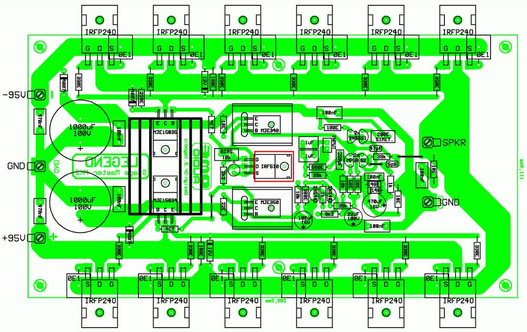
500W amplifier driver layout SHEMS

500W RMS Power Amplifier Based MOSFET Circuit Scheme

Pin on Audiophile

3kW Power Amplifier Driver Circuit Power amplifiers

Building Amplifier 1500W circuit at home

stk amplifier circuit diagram stk4101 Electronics Help

Pin on โปรเจกต์น่าลอง

PCB layout super OCL 500 Watt Power Amplifier Circuit
500W amplifier driver layout SHEMS


Pin oleh Islamrobiul di ডগহত Rangkaian elektronik
500W amplifier driver layout SHEMS


Electronic Circuit
1000W Driver Power Amplifier Namec TEF Electronic

2n3055 amplifier board circuit diagram YouTube


